Break Into Chip Design
Skill N Success
For ECE & EEE students and early-career engineers in India

Break into chip design in 90 days

A career roadmap built around real labs. Write Verilog, catch a real bug, simulate analog circuits, and learn what chip companies check when they hire. Start with a free chapter you can finish in one evening.

  • Pre-launch ₹499
  • Launch ₹999 · US$19
  • Sprint winners 12% off
Photo: Pexels
85,000chip-design engineers India aims to train under Chips to Startups
5,000direct jobs expected at peak at Micron's Sanand chip-packaging plant
₹6–12 LPAtypical fresher range for RTL and physical design roles in India
₹0spent on tools: every lab runs on free software
53-second lab tour · sound on

See the four labs before you sign up

Two digital labs and two analog labs, each with the real output a simulator printed. No stock screenshots.

A breadboard circuit with jumper wires next to a digital multimeter on a workbench.
The bench version: every simulation in the book has a cheap breadboard experiment you can try.
From design to factory to package

Every box is a team. Every team is a job title.

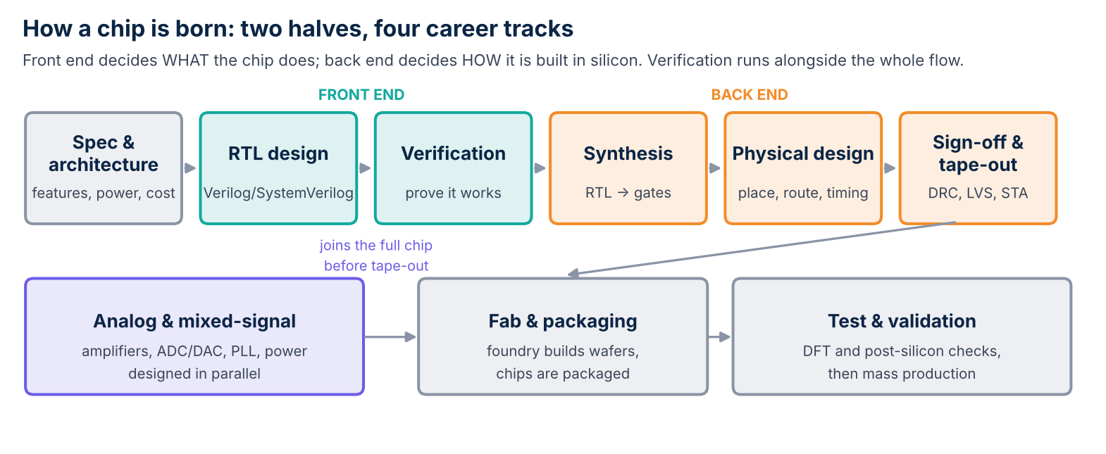
Engineers design the chip in software. A fab prints it onto silicon wafers. Packaging plants cut, mount, connect and test each chip. India is building all three, and each stage hires engineers.

Chip flow: spec, RTL design, verification, synthesis, physical design, sign-off and tape-out, then fab and packaging, then test; analog designed in parallel.
1 · WaferA silicon wafer covered in a grid of iridescent chip dies.

Hundreds of chips per wafer

A fab builds every chip on the wafer at once, layer by layer.
2 · Die attachTweezers placing a small black chip onto a green circuit board.

Cut, mount, connect

Each die is cut out, mounted, and wired or bumped to its package.
3 · PackageClose-up of a packaged computer chip on a printed circuit board.

Sealed, marked, tested

The package protects the die, carries heat away, and links it to the board.
4 · Assembly lineRows of electronic circuit boards in a production setting.

Into real products

Boards with the chips are built into phones, cars and servers.
India, 2026

Micron's ATMP (assembly, test, marking and packaging) plant in Sanand, Gujarat opened on 28 February 2026 to assemble and test DRAM and NAND memory, with about 5,000 direct jobs expected at peak. Packaging plants from Kaynes, CG Power and Tata (Assam) are next. Packaging and test need engineers who understand both the chip and the physics, which is why the book covers analog, test and DFT as well as digital.

Experiments inside the free chapter

Four labs. Real simulator output.

Every waveform and number below came from running the lab files with Icarus Verilog and ngspice. You get the same files, so you can reproduce each result on your laptop or in a browser.

LAB D1 · DIGITAL · RTL DESIGN

A 4-bit counter, and the test that proves it

Count 0 to 15, wrap to 0, and restart cleanly when reset fires mid-count. The testbench checks every clock edge against a reference model.

$ vvp sim RESULT: PASS - reset and rollover verified (25 checks)

What it proves to a recruiter: you write clean sequential logic and you test edge cases, not just the easy path.
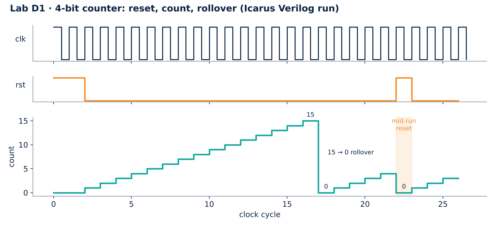
Waveform of clock, reset and a 4-bit count rising 0 to 15, rolling over to 0, and clearing on a mid-run reset.
LAB D2 · DIGITAL · VERIFICATION

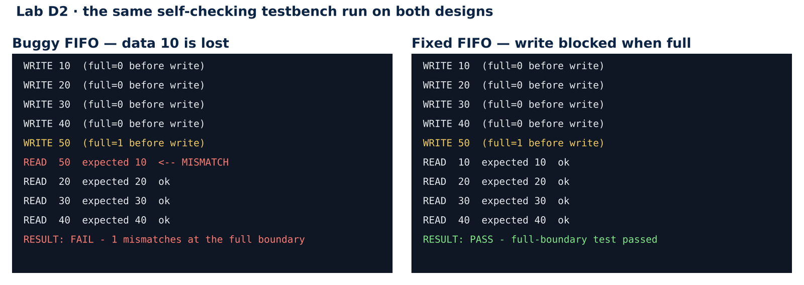
Find the hidden FIFO bug

A 4-entry buffer passes every normal test. Write five values into it and the buggy design silently overwrites the oldest one. One condition fixes it.

READ 50 expected 10 <-- MISMATCH RESULT: FAIL - 1 mismatches at the full boundary RESULT: PASS - full-boundary test passed (fixed)

Why it matters: this is the daily job of a verification engineer, the largest hiring track.

Two terminal logs: the buggy FIFO reads 50 where 10 was expected; the fixed FIFO passes.
LAB A1 · ANALOG · CIRCUITS

An RC filter where theory meets simulation

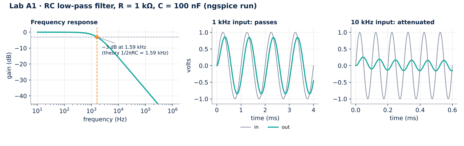
R = 1 kΩ, C = 100 nF. The formula 1/(2πRC) predicts a 1,591.5 Hz cutoff. The simulator measured it.

$ ngspice -b rc_lowpass.cir fc = 1.591551e+03 (1,591.6 Hz)

Where it lives: in front of every microphone, touchscreen and sensor that feeds an analog-to-digital converter.

Bode plot with the -3 dB point at 1.59 kHz, and time plots: a 1 kHz sine passes, a 10 kHz sine is strongly reduced.
LAB A2 · ANALOG MEETS DIGITAL · PHYSICAL DESIGN

Inside a logic gate: the CMOS inverter

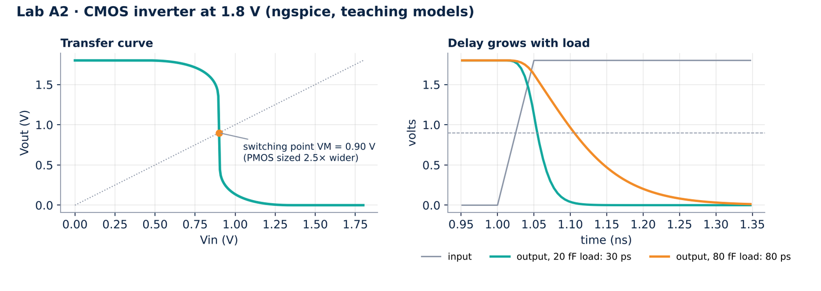
Every digital gate is an analog circuit. Balance the transistors and it switches at exactly half the supply. Make its load four times heavier and watch it slow down.

vm = 0.900 V tphl = 29.6 ps (20 fF load) tphl = 80.5 ps (80 fF load)

The bridge: this effect is what physical-design and timing engineers fight every day.

Inverter transfer curve switching at 0.90 V, and output transitions showing 30 ps delay at 20 fF and 80 ps at 80 fF.
Where your chips end up

Every lab maps to a product you use

A technician working on the circuit board of an opened smartphone.

Phones

An application processor, modem, power-management chip and camera sensor, each designed by separate teams.

RTL · verification · analog front ends
A charging cable plugged into an electric car.

Electric vehicles

Battery monitoring, motor control and radar chips, where precise analog and safety-checked digital logic meet.

Mixed-signal · power · test
Macro photo of a processor on a dark circuit board.

AI computing

Accelerator chips with billions of transistors, where timing closure and verification teams grow fastest.

Physical design · STA · verification
Quiz 1 · Find your track · 4 questions

Digital or analog? Pick by what you enjoy.

RTL design, verification, physical design and analog are four very different days at work. Answer four quick questions to see which fits you, and which lab to start with.

An engineer using a microscope to inspect a circuit board at an electronics bench.
Bench inspection: one of many skills shared by analog, test and packaging roles.
Jobs, pay and where demand is heading

What each track pays, and what companies check

TrackYour dayFresher pay in IndiaRecruiters check for
RTL designWrite Verilog for blocks: state machines, FIFOs, bus interfaces₹6–8 LPAVerilog, digital logic, clean synthesisable code
Design verificationBuild testbenches, hunt bugs, measure coverageTracks RTL designSystemVerilog, testbenches, OOP, Python or Perl
Physical design / STAFloorplan, place, route and close timing with scripts₹6–12 LPAStatic timing, DRC/LVS, Tcl scripting
Analog & mixed-signalDesign amplifiers, data converters, PLLs, power circuitsPremium over digital generalistsMOSFET and op-amp design, SPICE
Packaging & testAssemble, test and qualify chips at ATMP/OSAT plantsVaries by plant and roleTest basics, measurement, data analysis, DFT

Pay source: Futurense, chip design engineer salaries in India (2026). Top MNC offers run higher (Intel ₹18–24 LPA, NVIDIA ₹22–28 LPA including stock). Pay varies by city, company and skills. Hiring in India includes Intel, NVIDIA, Qualcomm, Texas Instruments, Samsung, AMD, TSMC and Saankhya Labs.

AI accelerators

Custom silicon for AI keeps verification and physical-design teams growing fastest.

Automotive and EV

Battery, motor-control and radar chips need analog and mixed-signal skills.

Chiplets and packaging

Chips built from smaller dies create roles in integration, test and signal integrity.

Low-power edge devices

Billions of battery devices keep low-power design and analog front ends in demand.

The 90-day plan

Four phases, each ending in a checkpoint you can show

About 10–12 hours a week. Students with exams can take the flexible pace of 5–7 hours a week and finish in about five months.

DAYS 1–21

Foundations

  • Logic, CMOS, timing
  • Verilog basics, first simulation
✓ 50 HDLBits problems + an FSM project
DAYS 22–49

Track deep dive

  • Verification, physical design or analog
  • Linux, Python, Tcl
✓ One track lab + one useful script
DAYS 50–77

Portfolio

  • Two projects, tested and written up
  • Waveforms and reports on GitHub
✓ 2 projects on GitHub with READMEs
DAYS 78–90

Get hired

  • CV, LinkedIn, outreach
  • 7-day interview sprint
✓ CV live, 20 applications, 1 mock interview
After day 90

Next phase of skilling: UVM and formal verification for DV, low-power and timing closure for physical design, data converters and PLLs for analog, and a tiny design on real silicon through a shared shuttle such as Tiny Tapeout.

Competition · Silicon Sprint

Solve 5 small design problems. Win 12% off.

Each problem is a small circuit or code snippet, the kind you meet in a first-round chip interview. The clock runs from your first problem.

  • Score 4 or 5 out of 5 to unlock code SPRINT12: 12% off the launch price (₹879 instead of ₹999, or US$16.72 instead of US$19).
  • Enter your sprint score with your sign-up. The fastest perfect scores each week get a shout-out on our Instagram.
  • One attempt counts per email. Calculator and paper allowed.
Quiz 2 · Chip IQ warm-up · 5 questions

How well did you read the labs?

A quick warm-up drawn from the four starter labs, with the reasoning shown after each answer.

The full book · Part 2 of the launch

Text, diagrams, lab output, audio and video in one kit

Each chapter follows the same pattern: a plain-English explanation, a real-world example, a lab you can run, a recruiter's view, and a five-question self-check.

20

Chapters

From how a chip works to your first offer, in five parts.

4+10

Labs and projects

Guided labs with expected outputs, plus 10 portfolio projects ranked by difficulty.

12

Audio summaries

5–8 minute recaps for revision on your commute.

10

Video lessons

Tool setup, coding, debugging and documenting a project.

150

Interview questions

Each with the reasoning, a common wrong answer and the likely follow-up.

1

Workbook

Track finder, 90-day tracker, evidence map, CV and README templates.

Free chapter today · full book at launch

Pre-order at ₹499, or start with the free chapter

Pre-launch, India₹499Pre-order now, until the full book launches.
Launch price₹999 · US$19India via UPI, cards and net banking (Razorpay). International via PayPal.
Silicon Sprint winners12% offCode SPRINT12 on the launch price: ₹879 or US$16.72.
Pre-order now · Pay ₹499

Secure checkout by Razorpay: UPI, cards, net banking and wallets. The book is emailed to you as soon as Part 1 is released. Changed your mind before delivery? Email debasis.panda1985@gmail.com for a full refund.

Engineering students learning circuit-board repair at an electronics workbench.

Silicon Sprint: not taken yet. Take it to qualify for 12% off.

We never share your details.

Questions

Before you sign up

Do I need paid tools like Cadence or Synopsys?

No. Every lab uses free software: Icarus Verilog, ngspice, Yosys and an open-source layout flow. The Verilog labs also run in a browser on EDA Playground, with nothing to install.

I'm in 2nd year. Is this too early?

It's a good time. The first phase covers digital logic, CMOS and Verilog basics, which line up with your coursework. Use the flexible pace of 5–7 hours a week.

Will this get me a job?

No book can promise that. It gives you a clear plan, real projects and practice for the questions companies ask. Your results depend on the work you put in and on each employer's needs.

Does it cover analog and packaging, or only digital?

All of them. Two of the four starter labs are analog, and the full book has chapters on analog and mixed-signal design, physical design and timing, DFT, test and post-silicon validation.

How does the ₹499 pre-launch price work?

Pre-order now for ₹499 through Razorpay (UPI, cards, net banking). The book is emailed to you as soon as Part 1 is ready, and you can ask for a full refund any time before delivery. After launch, the price is ₹999 in India and US$19 internationally.

Can I use the Sprint code with the ₹499 offer?

No. The 12% Sprint code applies to the launch price. The ₹499 pre-launch price is already the lowest price.